- Consumer Goods
- Healthcare
- Performance Materials
- Technology
-
Services
- Overview
- Sourcing
Sourcing
Accessing a global sourcing network.
- Market insights
Market insights
Generating ideas for growth.
- Marketing and sales
Marketing and sales
Opening up new revenue opportunities.
- Distribution and logistics
Distribution and logistics
Delivering what you need, when you need it, where you need it.
- After-sales services
After-sales services
Servicing throughout the entire lifespan of your product.
- Insights
- Home

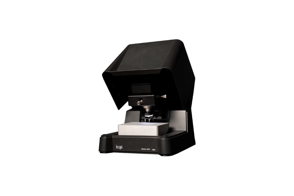
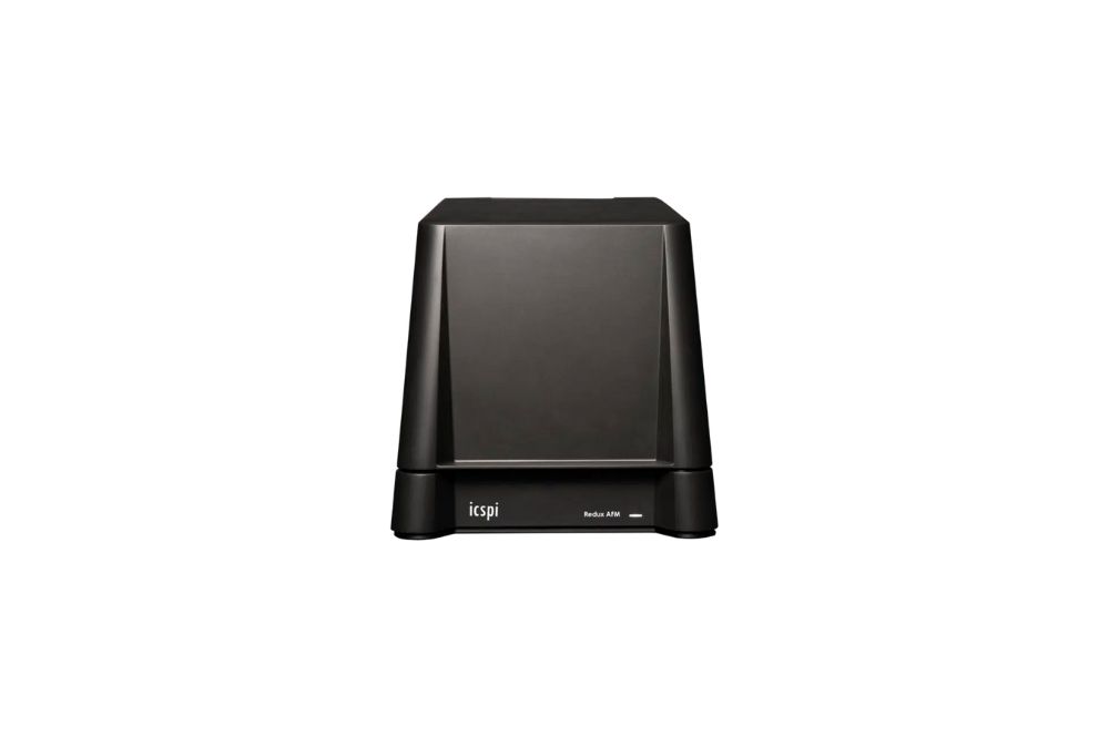
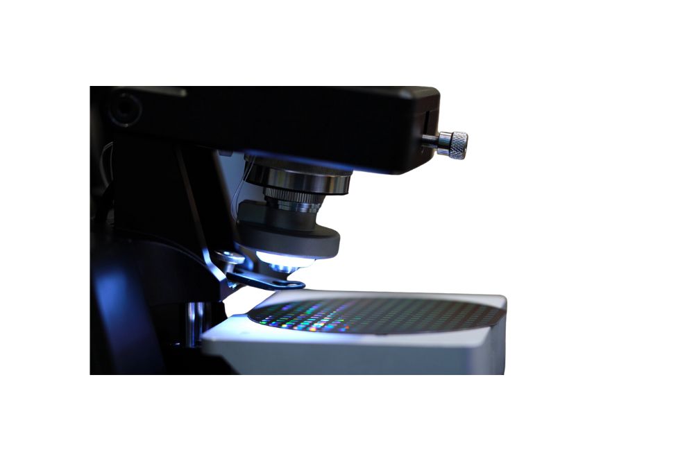
 ICSPI develops and produces easy to use and affordable benchtop AFM instruments designed for the individual scientist and individual lab to capture 3D images at the nanoscale. Incorporating our AFM-on-a-Chip technology, our flagship instrument, the nGauge AFM provides researchers and scientists 3D scans at the nanoscale in about a minute in their own lab and on their own bench. ICSPI is headquartered in Kitchener-Waterloo, Ontario, Canada.
