- Menu Close
- Consumer Goods
- Healthcare
- Performance Materials
-
Technology
- Overview
- Industries
- DKSH Indonesia products
Our products
Search our product database.
-
Services
- Overview
- Sourcing
Sourcing
Accessing a global sourcing network.
- Market insights
Market insights
Generating ideas for growth.
- Marketing and sales
Marketing and sales
Opening up new revenue opportunities.
- Distribution and logistics
Distribution and logistics
Delivering what you need, when you need it, where you need it.
- After-sales services
After-sales services
Servicing throughout the entire lifespan of your product.
- Insights
- Home
- Technology
- DKSH Indonesia products
- NTK Ceratec - Vacuum Chuck
- Home
- Technology
- DKSH Indonesia products
- NTK Ceratec - Vacuum Chuck


 NTK CERATEC's core business revolves around ceramics and solutions using ceramic materials based on the latest processing and coating technology. The characteristics of ceramics are developed, such as harmlessness, chemical stability, and heat tolerance and pursue ecology through high energy efficiency and energy saving performance in semiconductor and liquid crystal product manufacturing for various cutting-edge fields like electronics and industrial machines.
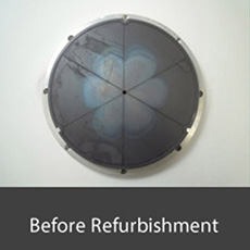